














Precision Laser Marking for Electronics and Semiconductors
A while back, I picked up a microchip from a failed circuit board and examined it under a loupe. On a surface barely 4mm by 4mm, the serial number was flawless—perfect spacing, sharp edges, and no visible heat damage to the surrounding material. The mark had been applied by a UV laser in under 50 milliseconds. That tiny chip had likely travelled through multiple countries—from fabrication in Asia to assembly and distribution—before ending up on a repair bench. And that single, precise mark made the entire journey traceable. That was the moment it became clear just how critical laser marking is in modern electronics manufacturing.

Across Australia’s electronics sector—from PCB assembly shops in Sydney to advanced manufacturing facilities in Melbourne—laser marking has become the standard method for component identification. Traditional methods like ink printing, adhesive labels, and pad printing simply don’t hold up under real production conditions. Electronics components are exposed to soldering temperatures exceeding 260°C, aggressive cleaning processes, humidity testing, and long-term field use. Laser marking stands out because it produces permanent, chemical-resistant marks that survive the entire lifecycle of the product.

What makes electronics marking particularly challenging is the scale and sensitivity involved. Components are often microscopic, and materials vary widely—from delicate polymers and ceramics to plated metals and silicon wafers. Even a slight excess of heat during marking can damage a circuit or compromise a semiconductor surface. At the same time, traceability requirements in industries such as automotive electronics, defence, and medical devices in Australia demand precise identification at every stage—from individual chips to fully assembled systems.

Traditional marking methods consistently fall short in these conditions. Ink-based markings can smear during soldering or fade under heat. Labels can peel off during cleaning or become trapped under protective coatings. Mechanical stamping introduces stress that can crack fragile components. In contrast, laser marking is a non-contact process that creates permanent marks instantly, without chemicals or physical force. It also achieves micrometre-level precision that conventional techniques simply cannot match.

In practical production environments, the benefits are immediate. For example, manufacturers that switch from inkjet marking to UV laser marking often see defect rates drop dramatically. Marks remain legible after soldering and cleaning, eliminating costly rework and improving quality control. For many businesses, it’s one of the simplest upgrades with the fastest return on investment.

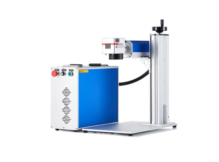
Different types of lasers are used depending on the material and application. UV lasers, operating at 355nm, are ideal for heat-sensitive components such as PCB substrates, IC packages, and ceramics. They work through a photochemical process rather than heat, meaning they can mark delicate surfaces without causing thermal damage. This makes them particularly valuable for high-precision industries like semiconductor manufacturing and LED production.

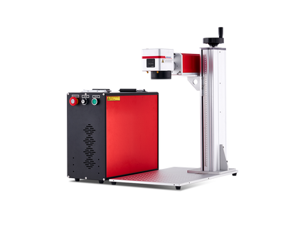
Fiber lasers, typically operating at 1,064nm, are the go-to solution for metal components. They are widely used to mark aluminium housings, stainless steel enclosures, copper connectors, and heat sinks. These systems produce high-contrast, durable marks at speeds suitable for production lines, making them a common choice for Australian electronics manufacturers working with metal assemblies and enclosures.
For more specialised applications, particularly involving plated components, MOPA fiber lasers offer a significant advantage. Their adjustable pulse duration allows precise control over heat input, which is critical when marking gold- or nickel-plated parts. This ensures the integrity of the plating—and therefore the electrical performance of the component—is preserved. In sectors such as telecommunications and high-reliability electronics, this level of control is essential.
Laser marking is used across a wide range of electronic components. Printed circuit boards require markings such as date codes, serial numbers, and compliance symbols that can survive the entire assembly process. UV lasers are commonly used here because they produce marks that resist soldering, cleaning, and coating processes while remaining clearly legible.
Semiconductor packages and IC chips present an even greater challenge due to their extremely small marking areas. Laser systems can produce high-contrast serial numbers and 2D codes on surfaces just a few millimetres wide, often in milliseconds. This speed ensures that marking does not become a bottleneck in high-volume production.
Surface mount devices (SMDs), which continue to shrink with each generation, require micromarking at an incredibly fine scale. Laser systems with spot sizes under 10 micrometres can mark components smaller than a grain of rice—something no traditional marking method can achieve reliably.
Connector terminals and lead frames often require selective removal of plating to improve solderability or create identification marks. MOPA lasers are particularly effective here, as they can remove thin plating layers without damaging the underlying metal. This eliminates the need for chemical etching and reduces process complexity.
Silicon wafers, used in semiconductor fabrication, require marking processes that introduce virtually no contamination. UV and green lasers are used to apply lot codes and alignment marks with minimal surface disruption, ensuring yield is not affected.
One of the most critical aspects of laser marking in electronics is thermal management. Unlike larger industrial parts, electronic components are highly sensitive to heat. A slight variation in laser parameters—such as pulse duration or power—can mean the difference between a clean, precise mark and a damaged component. This is why validated parameter settings, tailored to specific materials, are essential.
UV lasers address this challenge by using photochemical reactions rather than heat, resulting in an extremely small heat-affected zone. Meanwhile, MOPA systems provide precise control over pulse duration, allowing operators to minimise thermal impact when working with sensitive or plated materials.
For electronics manufacturers in Australia, integrating laser marking into production workflows also brings operational advantages. Modern systems can connect directly to ERP and MES platforms, enabling real-time serialisation and data tracking. This is particularly important in industries where compliance, traceability, and quality assurance are tightly regulated.
Ultimately, laser marking has become indispensable in electronics manufacturing because it solves a problem no other method can fully address. It delivers permanent, high-precision marks that survive harsh production environments, while maintaining the integrity of increasingly small and sensitive components. As Australian manufacturing continues to advance—particularly in sectors like defence, renewable energy, and medical technology—laser marking will remain a core technology for ensuring reliability, traceability, and product quality.