












What Is PCB Laser Engraving and What Can It Do?
I run a small electronics design studio—just three engineers, mostly working on power electronics and motor control boards. For years, we outsourced our PCB labelling. Every revision meant waiting on turnaround times, dealing with minimum order quantities, and losing flexibility during development. Eventually, we installed a fibre laser in the workshop. The first job we ran was a batch of 30 prototype boards, each requiring a unique serial number, a revision mark, and our company logo. The entire batch was completed in under an hour, and we had finished boards the same day they were assembled. Looking back, it’s hard not to think we should have made the switch much earlier.

Across Australia’s growing electronics sector—from small R&D labs to contract manufacturing operations—laser engraving for PCB and component labelling is becoming far more common than many expect. It’s not just a tool for large-scale semiconductor manufacturing. It’s equally valuable for prototyping, small-batch production, and even hobbyist-level PCB work. Whether you’re developing IoT devices, industrial controls, or custom embedded systems, laser marking offers a level of speed, precision, and permanence that traditional labelling simply can’t match.

At its core, PCB laser engraving is a non-contact process that creates permanent marks directly on the board surface. These marks can include serial numbers, date codes, revision identifiers, QR or Data Matrix codes, and company branding. Because the laser doesn’t physically touch the board, there’s no mechanical stress, and the markings remain intact through soldering, cleaning, and long-term use. This is particularly important in Australia, where electronics often operate in demanding environments—from mining equipment in Western Australia to outdoor systems exposed to heat, dust, and humidity.

It’s worth understanding that there are two distinct uses of lasers with PCBs. One is fabrication—using a laser to remove copper and form circuit traces. This is a specialised and complex process typically limited to advanced R&D environments. The more common and accessible application is labelling and marking, where lasers are used to add identification to finished or partially assembled boards. For most workshops and production environments, this second use case is where the real value lies.
In practical terms, laser marking covers a wide range of applications. Small workshops and makers often use fibre or CO₂ lasers for board labelling and branding. Electronics manufacturers rely on UV or fibre lasers for component identification and traceability. Contract manufacturers increasingly use laser-marked 2D codes to link each board to production data, test results, and quality records. Even prototype fabrication and depaneling can involve laser systems in more advanced setups.

Real-world experience backs this up. One small IoT company I spoke with—based in Brisbane—used to rely on adhesive labels for traceability. During assembly, labels would shift, fall off, or occasionally end up on the wrong board. After switching to a 30W fibre laser, they began marking each PCB with a serial number and 2D code before assembly. The marks now survive soldering and cleaning without issue, and they’ve had no traceability gaps since. As a bonus, the finished boards look far more professional when delivered to customers.
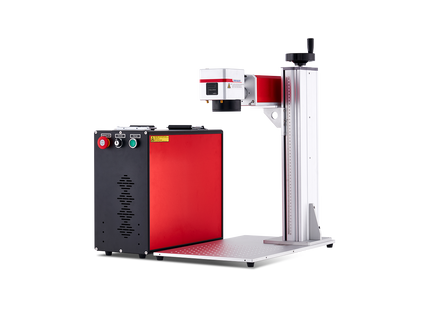
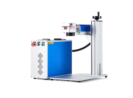
Choosing the right laser depends largely on the material and the stage of production. Fibre lasers are the most practical option for many Australian workshops, particularly when working with standard FR4 boards that have dark solder masks. These lasers create high-contrast marks by ablating or altering the surface layer, making them ideal for serial numbers, logos, and batch codes. They are fast, reliable, and integrate well with software like LightBurn for automated serialisation.

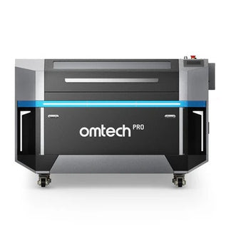
CO₂ lasers, on the other hand, are better suited for working directly with the PCB substrate or for cutting applications. They can mark lighter-coloured boards and are sometimes used in DIY fabrication workflows. However, they come with an important caveat. FR4 material releases hazardous fumes when engraved or cut with a CO₂ laser, including toxic compounds that require proper extraction systems. In Australia, workplace safety regulations make proper ventilation and filtration essential—this is not something to overlook.
For high-end or production-grade applications, UV lasers are the preferred choice. They produce extremely precise marks with minimal heat impact, making them suitable for marking assembled boards without risking damage to sensitive components. UV laser markings also withstand reflow soldering and cleaning processes, which is why they are widely used in professional electronics manufacturing environments.
For most workshops, the day-to-day workflow of PCB labelling is straightforward once the system is set up. Typically, the board outline is exported from design software such as KiCad or Eagle as a vector file. This file is then imported into LightBurn, where the marking layout is created. Variable text features allow automatic serial number generation, which is essential for batch production. Once parameters are calibrated for the specific solder mask colour, a simple fixture ensures consistent alignment for each board. After verifying the first sample, the rest of the batch can be processed quickly, with each board taking only seconds to mark.
The applications of laser marking in PCB work are broader than many expect. Date codes and revision marks are among the most valuable, allowing engineers and service teams to identify exactly when and how a board was produced. Logos and branding are commonly added to development boards, giving products a more professional appearance when presented to clients or investors. For production environments, 2D codes are increasingly essential, linking physical boards to digital records for full traceability.
Laser marking also plays a role in assembly. On complex prototype boards, marking component values or reference designators directly onto the PCB can significantly reduce assembly errors. This is particularly useful in R&D environments or when working with external assembly partners unfamiliar with the design.
As more Australian electronics businesses bring production capabilities in-house, laser engraving is proving to be one of the most practical upgrades available. It eliminates reliance on external suppliers for labelling, reduces turnaround times, and improves both traceability and product presentation. At the same time, it requires minimal consumables and integrates easily into existing workflows.
There are, however, some common mistakes to avoid. Using excessive laser power can damage the solder mask or underlying material. Marking directly over copper pads or traces can affect functionality. Failing to test parameters on scrap material often leads to inconsistent results. And when working with CO₂ lasers, inadequate fume extraction can create serious safety risks. Starting with conservative settings and refining through testing is always the best approach.
In the end, laser engraving for PCB and component labelling isn’t just a high-end manufacturing tool—it’s a practical, scalable solution for workshops of all sizes. Whether you’re building prototypes in a small lab or running batch production for commercial products, it offers a level of control, speed, and reliability that traditional methods simply can’t match.